
Chapter 6 of 14 · about 90 min
Layout with IHP PCells
The layout is what the factory builds. We draw it in KLayout with IHP’s parameterised cells (PCells): give a transistor its W, L and number of fingers and the PCell draws every layer correctly. We then connect the transistors with metal.
1. Open the layout editor
Select the cell opamp and press Layout (or FOSSLab > Open layout of this cell from the schematic). The first time FOSSLab asks to create the view: an empty opamp.gds with the top cell opamp. KLayout opens in editing mode with the SG13G2 technology: layers, grid, IHP’s menu SG13G2 PDK and FOSSLab’s menu.
2. Place the devices
- Instance (i), library SG13_dev, cell
nmosorpmos. In the PCell parameters setw(total width),landngexactly as in the schematic: LVS compares them. - The Miller capacitor: cell
cmim,Calculate = C,w = l = 24u. - Substrate and well contacts:
ptap1strips near the NMOS (to VSS),ntap1strips inside the N-well of the PMOS (to VDD). Rule LU.a/LU.b: no transistor may be more than 20 µm from a tap.
3. Connect
The PCells give the source/drain fingers in Metal1 but no gate contact: draw a GatPoly strap over the gate ends with contacts (Cont) and Metal1. Then route with Metal2 and Metal3, with vias (Via1, Via2). Finally put the pins: a Metal3 shape on the pin layer (Metal3.pin) and a text label with the net name (Metal3.text) for INP, INN, OUT, IBIAS, VDD and VSS. LVS uses the labels to match nets by name.
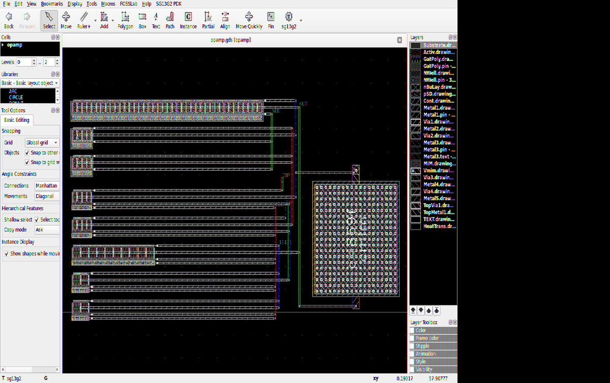
guard_ring). Run DRC, LVS and post-layout simulation after each change and compare the offset in Monte Carlo.The reference layout is generated by a script
The layout of the reference library was drawn by a Python script that uses the same PCells (app/fosslab/examples/opamp_layout.py in the FOSSLab folder). It is a good way to read how the layout is built: every rectangle has a comment. It reads the device sizes from examples/opamp.py (the MOS table and CC_SIDE), so after changing a size there, regenerate it with
$ fosslab example opamp --lib opamp_trywhich writes the whole reference library (schematic, symbol, testbenches with their setups, model and layout) as a new library opamp_try of your workspace.