
Chapter 7 of 14 · about 40 min
DRC and LVS
Two checks before any layout goes to the factory: DRC (is it manufacturable?) and LVS (is it the same circuit as the schematic?).
1. DRC
Save the layout, then in KLayout FOSSLab > Run DRC (IHP rules), or the DRC button of the Library Manager. A window shows the log and, at the end, the result: PASS: DRC clean, or the number of violations per rule. Show errors in KLayout opens the layout with the marker browser: click a rule, then a marker, and KLayout zooms to the error.
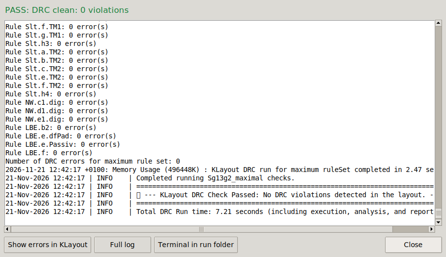
Errors you will meet: M1.b (two Metal1 shapes closer than 0.18 µm; often two shapes that should touch and miss by a few nm), LU.a/LU.b (a transistor too far from a substrate or well tap), Cnt.* and V1.* (contacts and vias too close to an edge of the metal around them). The reference layout went through exactly the first two before it was clean.
2. LVS
FOSSLab > Run LVS (KLayout or xschem) or the LVS button. FOSSLab netlists the schematic in LVS mode, extracts the layout with IHP’s LVS deck and compares them device by device and net by net.
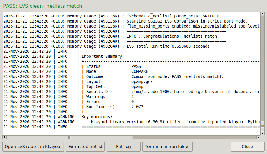
If they do not match, Open LVS report in KLayout opens the netlist browser: the circuits side by side, mismatching nets and devices in red; selecting one highlights it on the layout.
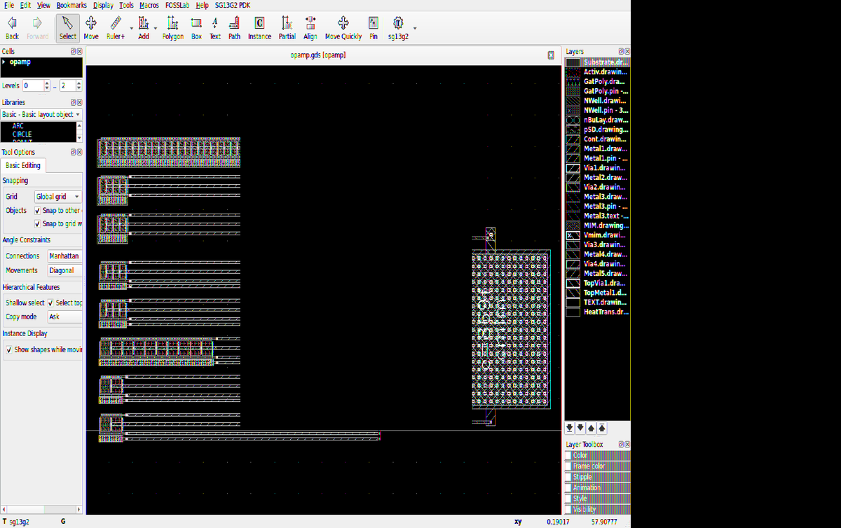
Typical causes: a missing pin label (the net gets a generated name), two nets shorted by a stray shape, a transistor whose ng or w differs from the schematic. Substrate and well taps are not compared: they are not drawn in schematics.
When both are clean, the cell list shows ✔ in the DRC and LVS columns.