
Chapter 3 of 14 · about 40 min
Schematic and symbol of the op-amp
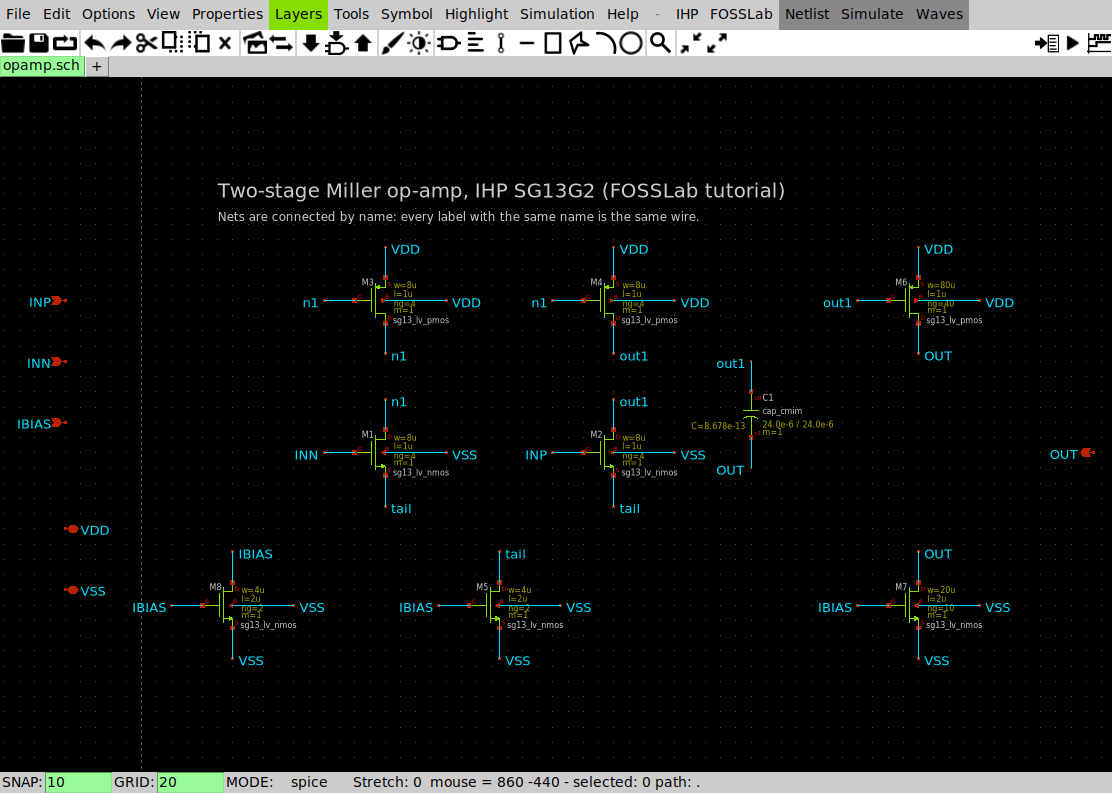
We create the op-amp: a library, a cell, its schematic with IHP SG13G2 transistors, and its symbol. The circuit is the two-stage Miller op-amp of Allen & Holberg, sized for SG13G2’s 1.2 V core transistors.
The specifications
| Specification | Target | Conditions |
|---|---|---|
| DC gain A0 | ≥ 55 dB | VDD = 1.2 V, CL = 1 pF, IBIAS = 10 µA, input common mode 0.8 V |
| Unity-gain frequency | ≥ 15 MHz | |
| Phase margin | ≥ 55° | |
| Slew rate | ≥ 10 V/µs | |
| Output offset (follower) | within ±5 mV | |
| Power | ≤ 100 µW |
The sizes
| Device | Role | IHP cell | W (fingers × width) | L |
|---|---|---|---|---|
| M1, M2 | input pair | sg13_lv_nmos | 8 µm (4 × 2 µm) | 1 µm |
| M3, M4 | current mirror (load) | sg13_lv_pmos | 8 µm (4 × 2 µm) | 1 µm |
| M5 | tail current source | sg13_lv_nmos | 4 µm (2 × 2 µm) | 2 µm |
| M8 | bias (diode) | sg13_lv_nmos | 4 µm (2 × 2 µm) | 2 µm |
| M6 | second stage | sg13_lv_pmos | 80 µm (40 × 2 µm) | 1 µm |
| M7 | second-stage current source | sg13_lv_nmos | 20 µm (10 × 2 µm) | 2 µm |
| C1 (Cc) | Miller compensation | cap_cmim | 24 µm × 24 µm (0.87 pF) | |
Why (W/L)6 = 10 (W/L)4? M7 carries 5 times M5’s current, i.e. 10 times M4’s. With M6 ten times wider than M4, M6’s gate sits at the same voltage as M4’s drain when both stages are balanced, so there is (to first order) no systematic offset.
1. A library and a cell
- Start the Library Manager (
fosslab). - File > New library…, name
opamp_tut. It appears under Workspace. - Select it and File > New cell… (or Ctrl+N): cell name
opamp, tick Schematic, OK. xschem opens on the empty schematic.
2. Draw the schematic
- Insert opens xschem’s symbol browser. From the library
sg13g2_prplacesg13_lv_nmos.symandsg13_lv_pmos.symfor M1 to M8, andcap_cmim.symfor C1. - Select each device and press q to set its properties:
w(total width),l,ng(number of fingers) from the table,m=1. For C1:w=24.0e-6 l=24.0e-6. - From the library
devices:ipin.symfor INP, INN, IBIAS,opin.symfor OUT,iopin.symfor VDD and VSS (set the name with q, propertylab). These pins are the cell’s interface. - Connect with wires (w), or with net labels (
lab_pin.sym): every label with the same name is the same net. The bulk of the NMOS goes to VSS, of the PMOS to VDD. - Save (Ctrl+s).
3. The symbol
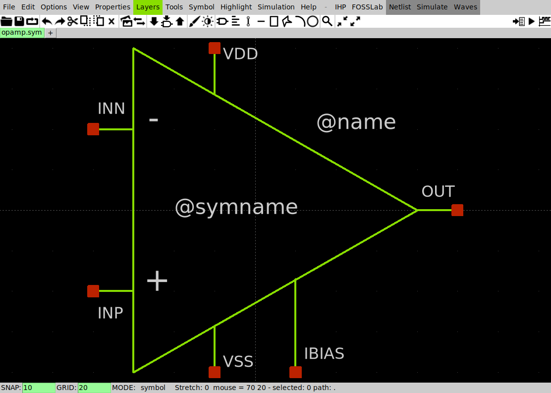
In xschem: FOSSLab > Create/update symbol from pins (or, in the Library Manager, right-click the cell > Create/update symbol from schematic pins). FOSSLab draws a box with the inputs on the left, the output on the right and the supplies on top and bottom. It is an ordinary xschem symbol: open it (Symbol button) and redraw it as the usual op-amp triangle if you like; keep the pins.
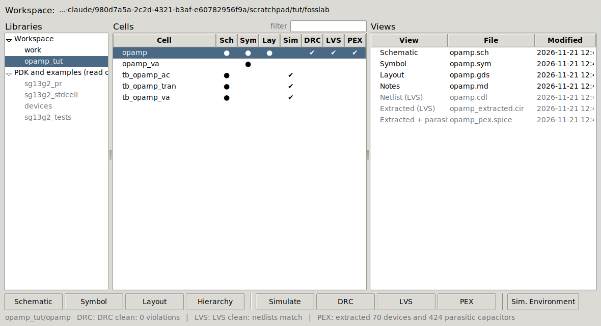
opamp_tut, cell opamp with its views. The dots show which views exist; the ticks, which checks passed.Stuck? Your teacher can share the reference library (
opamp_tut, read only). Right-click any of its cells > Copy cell… puts a copy in your own library.